-

Intellectual property verification
One is the verification of intellectual property rights. Through reverse engineering, the data on the PCB board can be collected and analyzed to provide evidence for legal disputes involving intellectual property infringement.
-
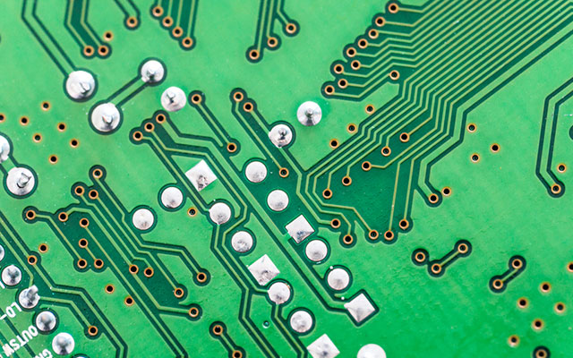
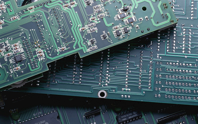
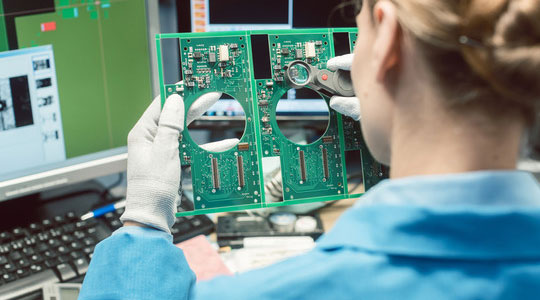
PCB Scanning
The next step is to scan the circuit board. Our experienced engineers use the most advanced scanning technology to accurately capture every detail of your PCB, including component placement and routing.
-
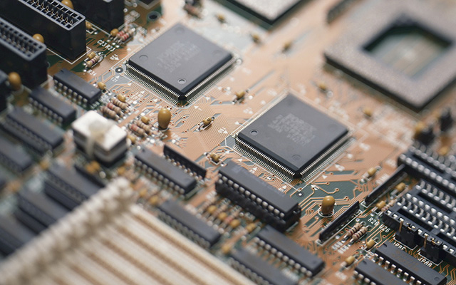
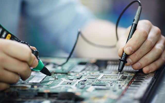
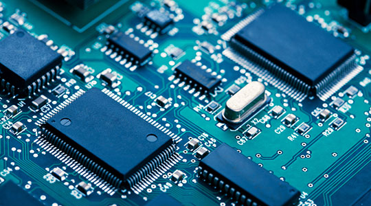
Reverse Analysis
After scanning, our engineers use their expertise to analyze the components, circuit routing, and other data from the scanned PCB. During this process, we thoroughly verify each component and its related parameters to ensure that they are all accurate and up-to-date.
-
Generate Files
The fourth step is to generate the necessary files for the revised PCB. Our engineers use the latest CAD tools and software to create a complete set of engineering files, including Gerber, PDF, AD, BOM files, schematic diagrams, and more.
-
Build Prototype
The fifth step is to build the model, and engineers use the reverse engineering technology generated by the PCB file to create a prototype of the circuit board. Once completed, we then conduct relevant tests to verify that the reverse engineering process was successful and error-free.
-
PCB Reverse Engineering Resource
Discover how to reverse engineer a printed circuit board (PCB) with our experts and get the most out of your PCB reverse engineering process.
 Home PCB
 Automotive
 Compute & Storage
 Energy &Industrial
 Capital Equipment
 Smart Home
 Medical Healthcare
 Packaging
 Telecommunications
 Camera PCB
 Transportation
 Printing
 Electronics